LED products are widely used in the fields of lighting and display by virtue of their outstanding advantages. LED chip as the core component of LED products directly determines product quality and its market competitiveness. Moreover, the quality of LED chips is jointly affected by their substrate, epitaxy and structure.
1. Substrate of LED chips: Laying the foundation for chips
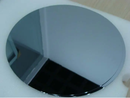
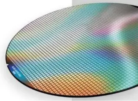
The substrate is the base of LED chips and is a wafer made of semiconductor materials. It is not only the key to affecting the epitaxial layer of the chip but also an important factor in determining the performance of the chip. Therefore, the selection of substrate materials is the primary consideration in making LED chips.
Comparison of main substrate materials:
- Sapphire (Al₂O₃): Sapphire substrates have the characteristics of high hardness and strong chemical stability, enabling them to provide a stable support structure for the epitaxial layer. At the same time, sapphire substrates are not easy to react chemically with other substances, ensuring the stability of LED chips in high-temperature, high-humidity and other environments. However, its thermal conductivity is relatively poor, which is not conducive to the dissipation of heat generated during the operation of the chip, thus affecting the performance and lifespan of the chip.
- Silicon carbide (SiC): Silicon carbide substrates have excellent thermal conductivity and can effectively improve the heat dissipation performance of chips. Moreover, its lattice constant is relatively matched with epitaxial layer materials such as gallium nitride (GaN), so that the epitaxial layer grown on it has high quality, which is beneficial to improving the luminous efficiency and reliability of LED chips. However, the cost of silicon carbide substrates is relatively high, which limits its large-scale application to a certain extent.
- Silicon (Si): Silicon materials are widely used in the semiconductor industry, and its preparation process is already very mature. This makes the production cost of silicon substrates relatively low. However, the lattice constant mismatch between silicon and epitaxial materials such as gallium nitride is relatively large, and special technologies need to be adopted to avoid introducing many crystal defects when growing the epitaxial layer.
2. Epitaxy of LED chips: The key to electro-optical conversion
The LED epitaxial layer refers to the semiconductor thin film grown by the epitaxy process on the substrate. The N-type and P-type semiconductors contained therein are the key to the luminescence of LED chips, and different epitaxial materials determine the different luminescence characteristics of the chips.
Characteristics of Common Epitaxial Materials:
- Gallium Nitride (GaN): Gallium nitride is a wide-band-gap semiconductor material. Its band-gap width enables it to emit light efficiently in the blue-green light band. In blue-green light chips, when electrons and holes meet and recombine in the active region of gallium nitride, photon energy corresponding to the blue-green light wavelength range is released. By controlling the growth conditions and doping elements of the gallium nitride epitaxial layer, the emission wavelength can be precisely adjusted to achieve continuous light emission from blue to green light.
- Gallium Arsenide (GaAs): Gallium arsenide is a compound semiconductor material. Its material properties make gallium arsenide have a relatively high luminous efficiency in the red-light band. Similarly, in red-light chips, when the electrons and holes in the gallium arsenide epitaxial layer recombine, it can effectively convert electrical energy into red-light emission.
3. Chip Structure: Shaping to Meet Requirements
With the development of industry technology, LED chips also vary in overall structural design according to different requirements.
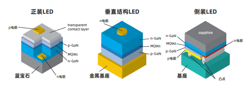
Face-up Structure
- Electrode Position: The electrodes are located on the same side above the chip. In this structure, current is injected from the electrode above the chip, passes through the active region, and then flows out from the other-side electrode.
- Relationship between Active Region and Substrate: The active region (usually the area where the P-N junction is located and is the key part for light emission) is above the substrate. After the light is emitted from the active region, it needs to pass through the electrode above the chip and the packaging material before it can be emitted.
Flip Structure
- Electrode Position: Contrary to the face-up structure, the electrodes are at the bottom of the chip. This structure is formed by flipping the face-up chip so that the active region is closer to the packaging material.
- Relationship between Active Region and Substrate: The active region is also above the substrate, but the flip structure reduces the light blocking by the electrodes by placing the electrodes at the bottom. At the same time, the distance between the chip and the packaging material is closer, which is beneficial for light extraction.
Vertical Structure
- Electrode Position: The electrodes are located on the top and bottom surfaces of the chip respectively, and the current flows perpendicular to the chip surface. One electrode is on the substrate side, and the other electrode is on the upper surface of the chip (the side opposite to the active region).
- Relationship between Active Region and Substrate: The active region is sandwiched between the upper and lower electrodes. This structure enables the current to pass through the active region vertically, and the substrate also participates in the current conduction process, which is beneficial for improving the uniformity of the current.


