Discussion on COB Package – By NovaStar Innovation
1. Characteristics of COB package
COB means Chip on Board, COB packaging is chip directly fixed on pcb board technology.
With most concerns of display effect, either sealing or filming can ensure COB surface has a qualitative leap for LED screen uniformity and contrast.
COB packaging makes LED panel luminescence tend to be surface light source, which also makes COB screen applied for camera shooting, to a large extent avoid phenomenon of moore grain.


In addition, large screen applications based on COB put forward higher requirements for field installation, all that needs to maintain a high degree of consistency and smoothness. Secondly, dead lights and other issues of COB screen body become little, once it occurs, using laser or polishing panel surface to do maintenance is a problem.
2. Characteristics of COB package in LED manufactory
Since 2023, display industry invests a lot more in COB, traditional LED panel manufactories have accelerated production line layout as well.
In the exploration of Mini & MicroLED display technology route, COB is not the unique new one, but the most important approach for everyone.
3. Characteristics of COB package in the industry chain
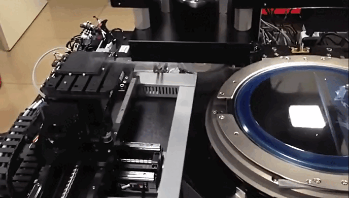
Different from traditional SMD, COB manufacturing eliminates RGB wick packaging link. RGB light-emitting chip is directly taken from wafer then fixed on pcb board to complete crystallization process. For the whole COB industry chain, light-emitting chip packaging link is omitted, no more light-emitting pixel mixing, which causes problem of initial uniformity of COB panel, making COB calibration an essential process rather than icing on the cake.

Technology innovation always bring surprise to the industry development. Speaking of COB “mixed lamp” effect, light-emitting chip is randomly taken out from different wafers and random die bonding is placed on pcb’s different area, which where the poor initial display uniformity comes.
4. Characteristics of COB Package in the market
COB display becomes more popular globally. Gifts in nature bring better market share. Cost for P1.5 and below is exceedingly competitive with SMD at the same pixel pitch, even lower.
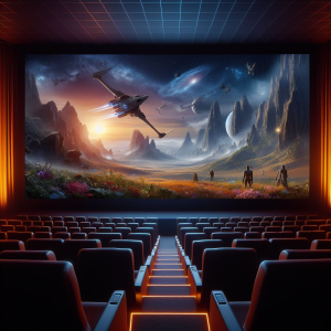
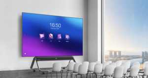
For certain application, such as all-in-one, control room, education venues, home theater, shooting and etc, integrators and end users prefer COB for high end projects, meanwhile, business clients have been winning more bids with COB proposal.
All these constantly helps broaden the application boundaries of COB display.

Once more projects seen, definitely a rapid growth of COB will be a big role playing in the market.
See you all next page.
NovaStar Innovation